

Contents

Source: MDPI
Designing Multilayer Optical Devices: A Comprehensive Guide
Introduction
Multilayer optical devices play a crucial role in various optical applications, including laser mirrors, anti-reflection coatings, and optical filters. The design of these devices requires careful consideration of various parameters to achieve the desired optical properties. This article explores the strategies and methodologies involved in designing multilayer optical devices.
Understanding Design Goals
The initial step in designing a multilayer optical device is to establish clear design goals. This involves defining the specific optical properties that the device should exhibit. A common practice is to use a figure of merit (FOM) to evaluate the design’s performance. The FOM is a quantitative measure that helps in assessing how well the design meets the desired specifications. Ideally, the FOM should be zero for a perfect design, with deviations incurring positive penalties.
Initial Configuration and Material Selection
Choosing the appropriate materials is a critical aspect of the design process. The selection is often constrained by the availability of materials and the required properties. Designers must also consider constraints related to the number of layers and total coating thickness. The decision to start with an initial design or to rely entirely on numerical optimization depends on the specific requirements of the project.
Designing Anti-reflection Coatings
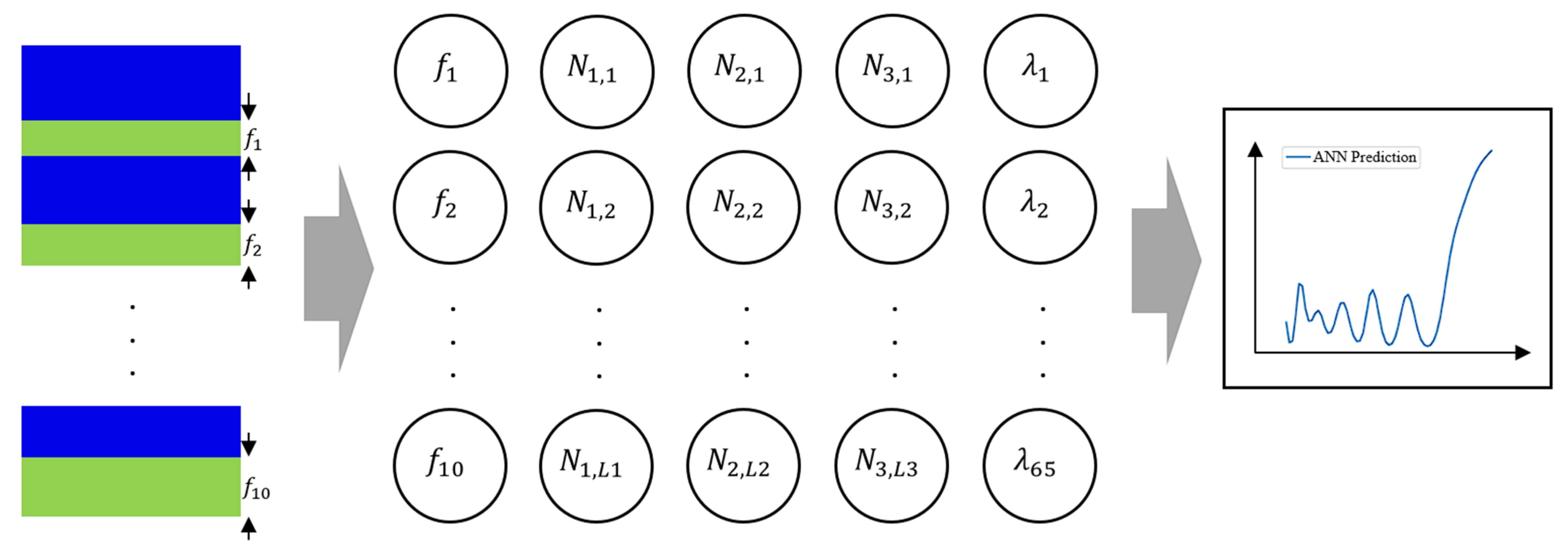
Anti-reflection coatings are designed to minimize reflections at specific wavelengths. A simple design may involve a single layer with a refractive index close to the square root of the substrate’s index. More complex designs require multiple layers and numerical optimization to achieve low reflectance across a range of wavelengths and angles of incidence. Techniques such as Monte-Carlo algorithms are often employed to explore the parameter space and identify optimal designs.

Designing Laser Mirrors
Laser mirrors are typically designed to provide high reflectance over a specific wavelength range. Bragg mirrors, consisting of alternating layers of two materials, are a common choice. The design process involves checking the mirror’s performance across different wavelengths and angles, with local optimization used to refine the design.
Dichroic Mirror Design
Dichroic mirrors are more complex, requiring specified properties at two different wavelengths. A common approach is to use a short-pass filter design, which involves modifying a Bragg mirror structure to achieve low reflectance in certain regions. Numerical optimization is essential to fine-tune these designs.

Double-chirped Mirrors
The design of double-chirped mirrors is particularly challenging due to the need for specific wavelength-dependent group delay dispersion and high reflectance. This involves varying the Bragg wavelength within the structure and modulating the layer thickness ratios. Efficient optimization often requires reducing the number of parameters to be adjusted, focusing on key aspects like chirp and duty cycle modulation.
Conclusion
Designing multilayer optical devices is a complex process that requires a clear understanding of design goals, careful material selection, and the use of advanced optimization techniques. Whether designing simple anti-reflection coatings or sophisticated double-chirped mirrors, the flexibility of design software and a well-defined figure of merit are crucial for achieving optimal results.
Source: MDPI
Feel free to comment your thoughts.

Author
Experienced laser technology expert with years of experience working in both industrial and academic landscapes. Adept at leveraging business acumen and scientific skills to drive innovation and achieve breakthrough results. Aiming to further advance the realm of laser technology and its applications.

