

Contents

Source: Fiberopticx
Understanding p–i–n Photodiodes: Design, Advantages, and Applications
Introduction to Photodiodes
Photodiodes are semiconductor devices that convert light into electrical current. They play a crucial role in a variety of applications, including optical communication systems, light detection, and measurement systems. Among the different types of photodiodes, the p–i–n photodiode is particularly significant due to its unique structure and enhanced performance characteristics.
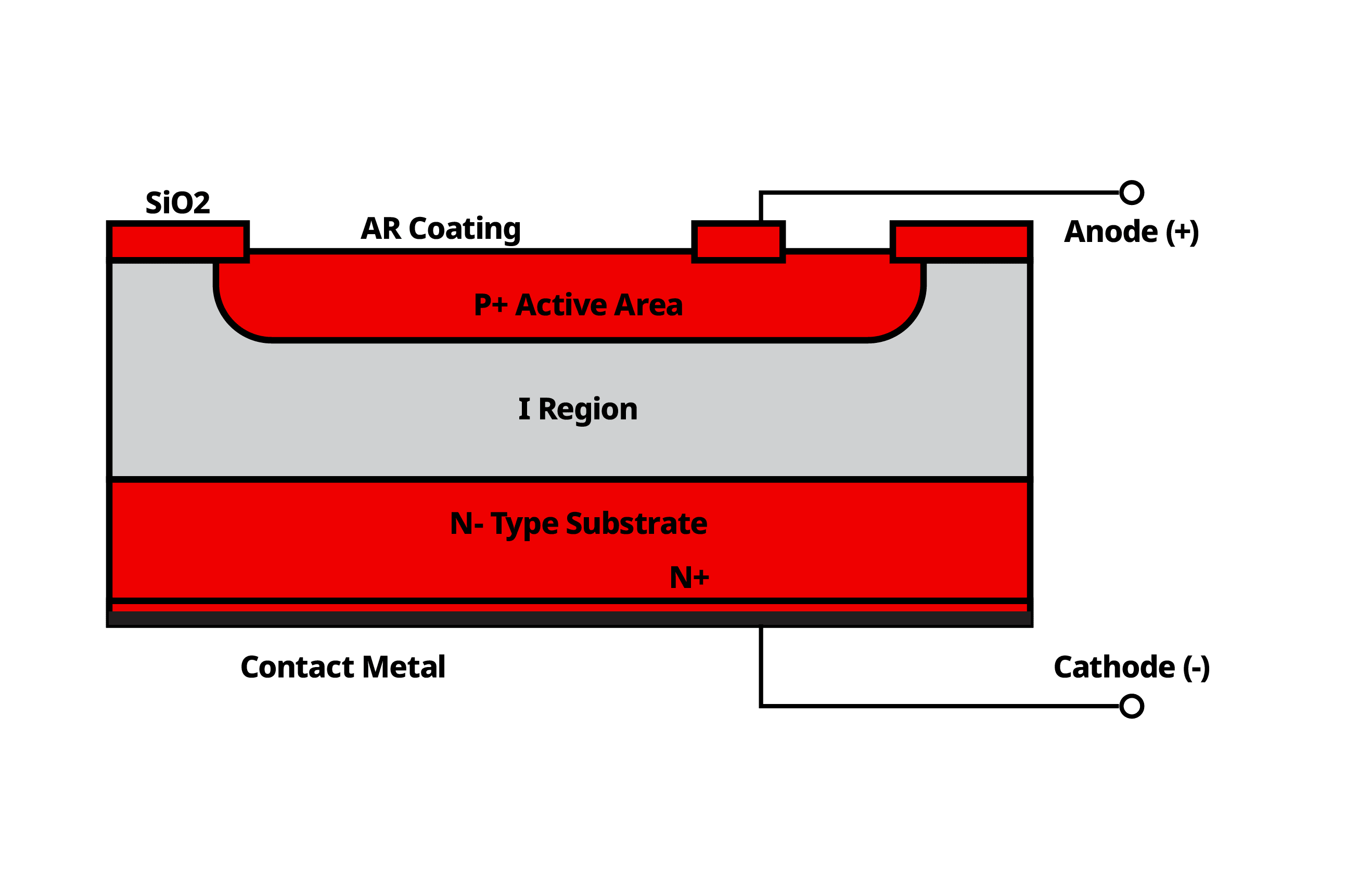
What is a p–i–n Photodiode?
A p–i–n photodiode is a type of photodiode that includes an intrinsic (i.e., undoped) layer sandwiched between the p-type and n-type semiconductor regions. This intrinsic layer is crucial as it absorbs most of the incident photons, leading to the generation of electron-hole pairs that contribute to the photocurrent. The structure of a p–i–n photodiode allows for efficient light absorption and carrier collection, making it suitable for high-speed and high-sensitivity applications.
Advantages of the p–i–n Design
The p–i–n photodiode offers several advantages over traditional p–n photodiodes:
- Increased Quantum Efficiency: The intrinsic layer is typically thicker than the depletion region in a p–n photodiode, allowing for more complete absorption of photons and generation of carriers within this layer.
- Higher Detection Bandwidth: The reduced capacitance due to the intrinsic layer enhances the detection bandwidth, making p–i–n photodiodes suitable for high-frequency applications.
- Improved Speed: With most carriers generated in the intrinsic region, the p–i–n photodiode exhibits faster response times, minimizing signal distortion and improving performance in high-speed optical communication systems.
Materials Used in p–i–n Photodiodes
Different semiconductor materials can be used to construct p–i–n photodiodes, each offering specific benefits:
- Silicon: Widely used for its sensitivity to visible and near-infrared wavelengths, silicon p–i–n photodiodes are cost-effective and offer good performance for numerous applications.
- Indium Gallium Arsenide (InGaAs): Suitable for detecting longer wavelengths up to 1.7 μm, InGaAs photodiodes are favored in applications requiring extended spectral response, although they are generally more expensive.
- Germanium: An alternative to InGaAs, germanium p–i–n photodiodes are less costly but exhibit slower response times and higher dark currents.
Applications of p–i–n Photodiodes
p–i–n photodiodes are utilized in a variety of applications due to their high-speed and high-sensitivity characteristics. They are commonly found in optical communication systems, where they serve as receivers capable of handling high data rates, sometimes exceeding 100 Gbit/s. Additionally, they are used in laser synchronization, pulse measurement, and other precision optical measurements.
Conclusion
The p–i–n photodiode is a vital component in modern photonics, offering enhanced performance through its unique design. Its ability to efficiently convert light into electrical signals with high speed and sensitivity makes it indispensable in advanced optical systems. With ongoing advancements in semiconductor materials and fabrication techniques, the capabilities of p–i–n photodiodes continue to expand, further solidifying their role in the future of photonics technology.
Source: RS Components
Feel free to comment your thoughts.

Author
Experienced laser technology expert with years of experience working in both industrial and academic landscapes. Adept at leveraging business acumen and scientific skills to drive innovation and achieve breakthrough results. Aiming to further advance the realm of laser technology and its applications.

