Contents
![]()
Source: ResearchGate
Exploring Orientation-patterned Semiconductors
Introduction to Orientation-patterned Semiconductors
Orientation-patterned semiconductors are a class of materials that offer unique properties for nonlinear frequency conversion processes, especially in the long-wavelength infrared spectrum. Unlike traditional dielectric materials, semiconductors like gallium arsenide (GaAs) exhibit a wider transparency range and higher nonlinear coefficients, making them ideal for applications such as optical parametric amplifiers and difference frequency generation.
Quasi-phase Matching in Semiconductors
Semiconductors often require quasi-phase matching (QPM) due to their inability to achieve traditional phase matching methods like periodic poling. Techniques like orientation-patterning have been developed to create a periodic pattern of domain orientation in semiconductors, allowing for efficient nonlinear conversion processes.
Applications and Devices
Orientation-patterned semiconductor devices have shown promising results in various processes, including second-harmonic generation, wavelength conversion, and optical parametric oscillation. Techniques such as the stack-of-plate method and epitaxial growth on patterned films have been utilized to create these devices with high efficiency and precision.
Future Prospects and Developments
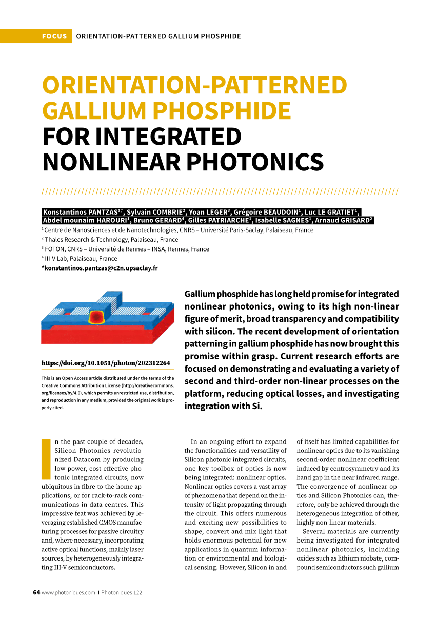
While gallium arsenide remains a popular choice for orientation-patterning, other semiconductor materials like gallium phosphide (GaP), ZnSe, and ZnTe have also shown potential for nonlinear optical applications. Advanced epitaxial techniques, including lithographic methods and heteroepitaxy, are continuously being developed to enhance the performance and versatility of orientation-patterned semiconductor devices.
Conclusion
Orientation-patterned semiconductors represent a promising avenue for achieving efficient nonlinear frequency conversion processes in the infrared spectrum. With ongoing research and advancements in fabrication techniques, these materials are poised to play a significant role in the development of high-performance optical devices for various applications in photonics and beyond.

Source: ResearchGate
Feel free to comment your thoughts.


