Contents

Source: Energy Education
Understanding Band Gaps in Optics and Photonics
Introduction to Band Gaps
Band gaps are fundamental in understanding the electronic and optical properties of materials. They play a crucial role in determining whether a material behaves as a conductor, semiconductor, or insulator. In solid-state physics, a band gap refers to the energy range in a solid where no electron states can exist.
Electronic Band Gaps
Dielectrics
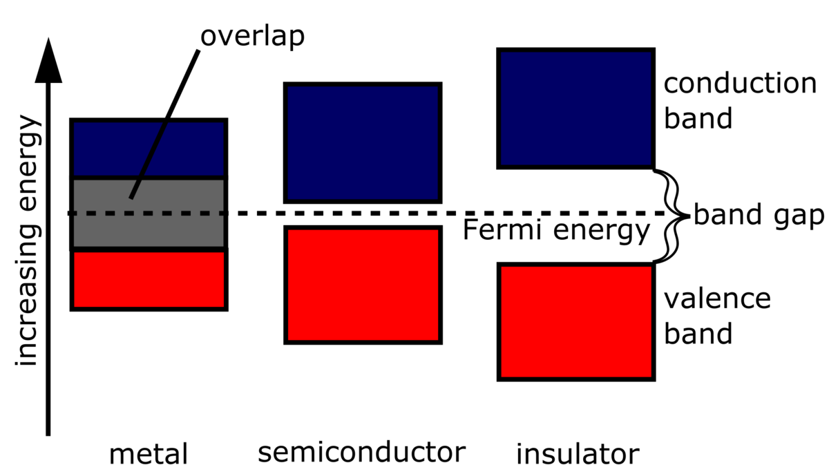
Dielectrics are materials with a large band gap, typically above 4 eV. This large gap means that all electronic states below the band gap are filled, and those above are empty, making these materials excellent insulators. They do not conduct electricity because there are no available states for electrons to move into under an electric field. Dielectrics are transparent to visible and near-infrared light because the photon energy is insufficient to bridge the band gap.
Semiconductors
Semiconductors have a smaller band gap, usually a few electron volts or less. This allows for some electrical conductivity as thermal energy can promote electrons from the valence band to the conduction band at room temperature. The band gap also determines the wavelengths of light the material can absorb and emit, making semiconductors crucial in electronic devices like diodes and transistors.
![]()
Metals and Semimetals
In metals, the Fermi energy lies within a band, allowing for easy electron movement and thus high electrical conductivity. Metals are typically reflective due to their ability to absorb and re-emit light. Semimetals have similar properties but with a lower density of states near the Fermi level, resulting in unique electronic characteristics.
Photonic Band Gaps
Photonic band gaps occur in materials with a periodic structure in their refractive index, preventing certain wavelengths of light from propagating through the material. This phenomenon is utilized in photonic crystals and fibers to control and manipulate light in advanced optical applications.

Applications and Importance
Band gaps are essential in designing various photonic devices. They determine the operational wavelengths of LEDs and laser diodes, the efficiency of photovoltaic cells, and the sensitivity of photodetectors. Band gap engineering, which involves adjusting the composition of semiconductor materials, allows for the customization of electronic and optical properties to suit specific applications.
Conclusion
Understanding band gaps is vital for advancing technology in electronics and photonics. By manipulating band gaps, scientists and engineers can develop materials and devices with tailored properties to meet the demands of modern technology.
This blog post provides an informative overview of band gaps in the context of optics and photonics, offering insights into their significance and applications. It is designed to be both educational and accessible, utilizing publicly available images to enhance understanding.

Source: Metallurgie Wissen – WordPress.com
Feel free to comment your thoughts.


